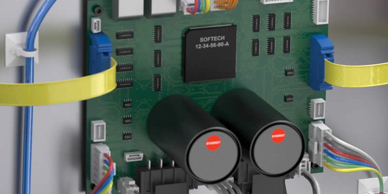
Printed circuit boards are essential to the electronics industry. PCBs are the backbone of most modern devices. They contain the resistors, capacitors, transistors, logic elements, memory chips, processors, and other system components. Their surfaces are made to ensure a good connection between each part so that adequate power is provided and that signals can go to their intended destinations. These can be created one at a time for prototyping or in millions for mass manufacturing. Below are the steps that make up the PCB manufacturing process:
1. Circuit Design
Before anything physical can be built, engineers will first have to design the circuit. They have a great deal of freedom in terms of style and methodology. Components can be laid out on a board in many ways. Multiple configurations can work, although some are more economical and robust than others. The higher the number of components, the greater the complexity of the circuits. They may have to be fine-tuned by specialists before getting the go signal for manufacturing.
2. Board Selection
Once the green light is obtained, board selection can begin. Most will default to FR4 which is made from low-cost glass fiber. It is temperature-resistant, durable, and easy to work with. If budget is an issue, then a cheaper type of board may be chosen for the project. If performance is the main priority, then PTFE boards could be the best bet. The surfaces of the board will usually have copper cladding for excellent conductivity.
3. Chemical Etching
The circuit design must first be transferred to the copper surface. This is usually accomplished by chemical etching. The desired pattern is printed onto a transparent sheet to serve as a mask while the copper is covered with photo-resist material. With exposure to UV light, parts of the photoresist will wear off and the image on the mask will be duplicated onto the PCB. This will then be submerged into ferric chloride for etching. Copper in any area that isn’t covered will be stripped away.
4. Automated Milling¬
Chemical etching is the primary process for this stage of development but it is not the only way to go. It is also possible to use mechanical means of transferring the design onto the board. This will require a very accurate milling machine given the low margin for error. Computer-controlled machines are necessary to maintain high accuracy while removing the unwanted copper. This tends to be slower than chemical removal so it is only suitable for small batches.
5. Drilling
Sections of the PCB may require holes to fasten the board onto the chassis using screws and the like. Sometimes holes can also serve as connections from the top layer to the bottom layer in complex circuit designs. These may also contain a copper layer for conductivity. In order to lower the cost of manufacturing, most holes are created with the same drill size.
6. Soldering
A layer of solder resist can be added onto the board to protect areas from short circuits and unwanted signals. This can often be identified by its green color. Components can then be soldered using lead or gold. The latter is good for longevity and reliability as gold does not tarnish while providing excellent conductivity.
7. Printing
Finishing touches include silk screen printing of text, symbols, and other things on the surface. These will help technicians later on in case they need to troubleshoot problems or replace faulty components. The prints will minimize confusion and boost the speed of quality control activities.
Most companies, like Avanti Circuits will design the circuit and then outsource the PCB manufacturing process to specialists for financial and technological benefits.